From October 9 through October 12, the autumn school on electron microscopy in materials science took place at the Harnack House in Berlin. This school offered both practical courses as well as lectures on different aspects of modern electron microscopy.
Time: Monday, Oct 9, 9:00 am until Thursday, Oct. 12, 18:00
Sponsors:
Programme:
Monday, Oct 9, 2017 |
|
| 09:00-09:45 | „Koch_AutumnSchool_Intro_InlineHolography“ (C. Koch, HUB) Download slides |
| 09:45-10:00 | Coffee break |
| 10:15-11:00 | „Off-axis electron holography“ (T. Niermann, TUB) Download slides |
| 11:00-11:45 | „Applications of off-axis electron holography“ (M. Lehmann, TUB) Download slides |
| 12:00-13:00 | Lunch |
| 14:00-14:45 | „FIB TEM-lamella preparation: From standard to heating and electrical measurements“ (D. Berger, TUB) Download slides |
| 14:45-15:30 | „Strain Mapping in Reciprocal and Real Space“ (M. Albrecht, IKZ) |
| 15:30-16:00 | Coffee break |
| 16:00-16:45 | „Mathematical Foundations of Tomography“ (W. Van den Broek, HUB) Download slides |
| 16:45-17:30 | „Application of tomography to semiconductor heterostructures“ (A. Trampert, PDI) |
| 17:45-20:00 | Poster Session (list of posters) |
Tuesday, Oct 10, 2017 |
|
| 09:00-09:45 | „Focused ion and electron beam processing“ (K. Höflich, HZB) Download slides |
| 09:45-10:00 | Coffee break |
| 10:15-11:00 | „Correlative scanning electron microscopy for materials analyses“ (D. Abou-Ras, HZB) Download slides |
| 11:00-11:45 | „in-situ TEM and SEM“ (R. Farra / M. Willinger, FHI) Download slides by R. Farra, Download Slides by M. Willinger |
| 12:00-13:00 | Lunch |
| 14:00-17:30 | Lab Courses |
Wednesday, Oct 11, 2017 |
|
| 09:00-09:45 | „Scanning Transmission Electron Microscopy“ (P. Werner, MPI Halle) Download slides |
| 09:45-10:00 | Coffee break |
| 10:15-11:00 | „Inelastic scattering in the TEM“ (W. Hetaba ; FHI) Download slides |
| 11:00-11:45 | „Electron energy loss spectroscopy“ (W. Wollgarten, HZB) Download slides |
| 12:00-13:00 | Lunch |
| 14:00-17:30 | Lab Courses |
Thursday, Oct 12, 2017 |
|
| 09:00-09:45 | „Electron Crystallography“ (H. Kirmse, HUB) Download slides |
| 09:45-10:00 | Coffee break |
| 10:15-11:00 | „Structure analysis through the pair distribution function“ (E. Willinger, FHI) Download slides |
| 11:00-11:45 | „Mapping fields and strain by scanning precession electron diffraction“ (B. Haas, HUB) Download slides |
| 12:00-13:00 | Lunch |
| 14:00-17:30 | Lab Courses |
| 18:30-21:00 | BBQ |
Friday, Oct 13, 2017 |
|
| Departure | |
Detailed information about the laboratory courses on Tuesday, Wednesday, and Thursday is provided on a separate page.
This school was organized and run by members of the following institutions (in alphabetical order):
- Fritz-Haber-Institut der Max-Planck-Gesellschaft (FHI)
- Helmholtz-Zentrum Berlin für Materialien und Energie (HZB)
- Humboldt Universität zu Berlin (HUB)
- Leibniz-Institut für Kristallzüchtung (IKZ)
- Max-Planck-Institut für Mikrostrukturphysik (MµP)
- Paul-Drude-Institut für Festkörperelektronik (PDI)
- Technische Universität Berlin (TUB)
Financial support for this school is provided by
- German Research Foundation / Deutsche Forschungsgemeinschaft
- German Society for Electron Microscopy / Deutsche Gesellschaft für Elektronenmikroskopie
- Thermo Fischer Scientific
- Carl Zeiss
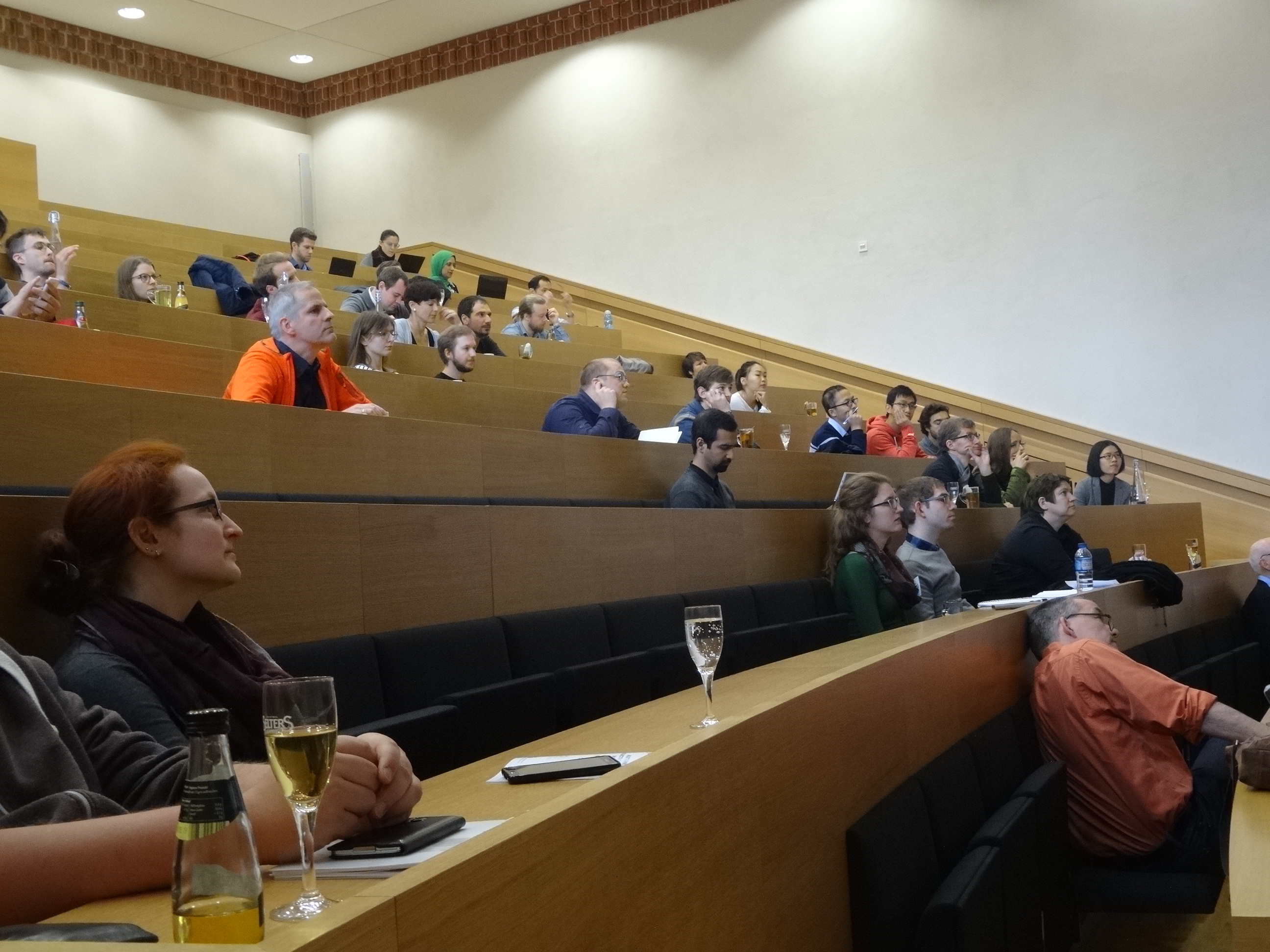
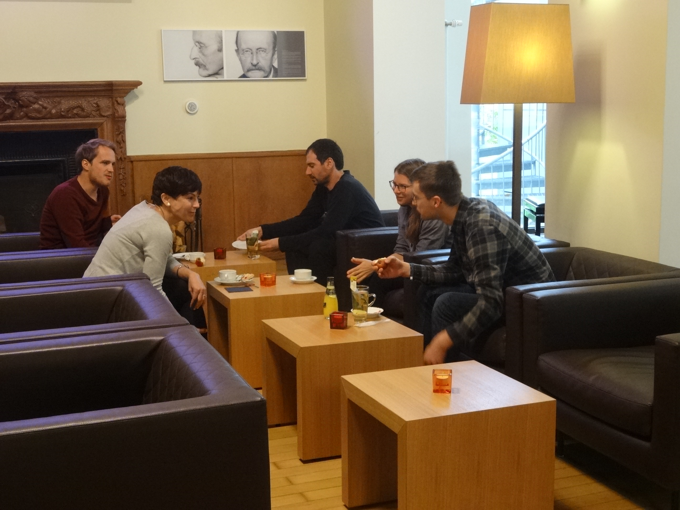
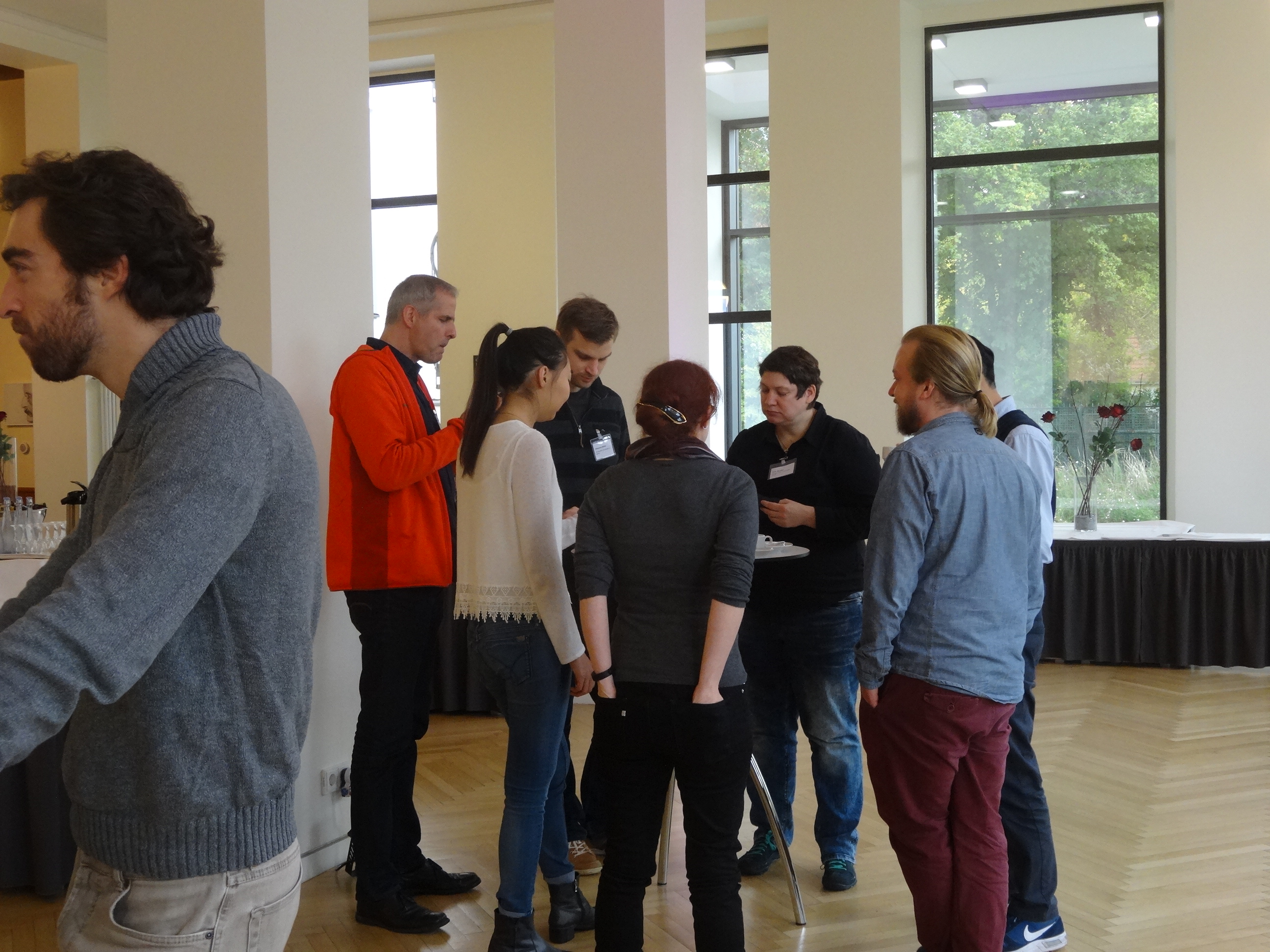
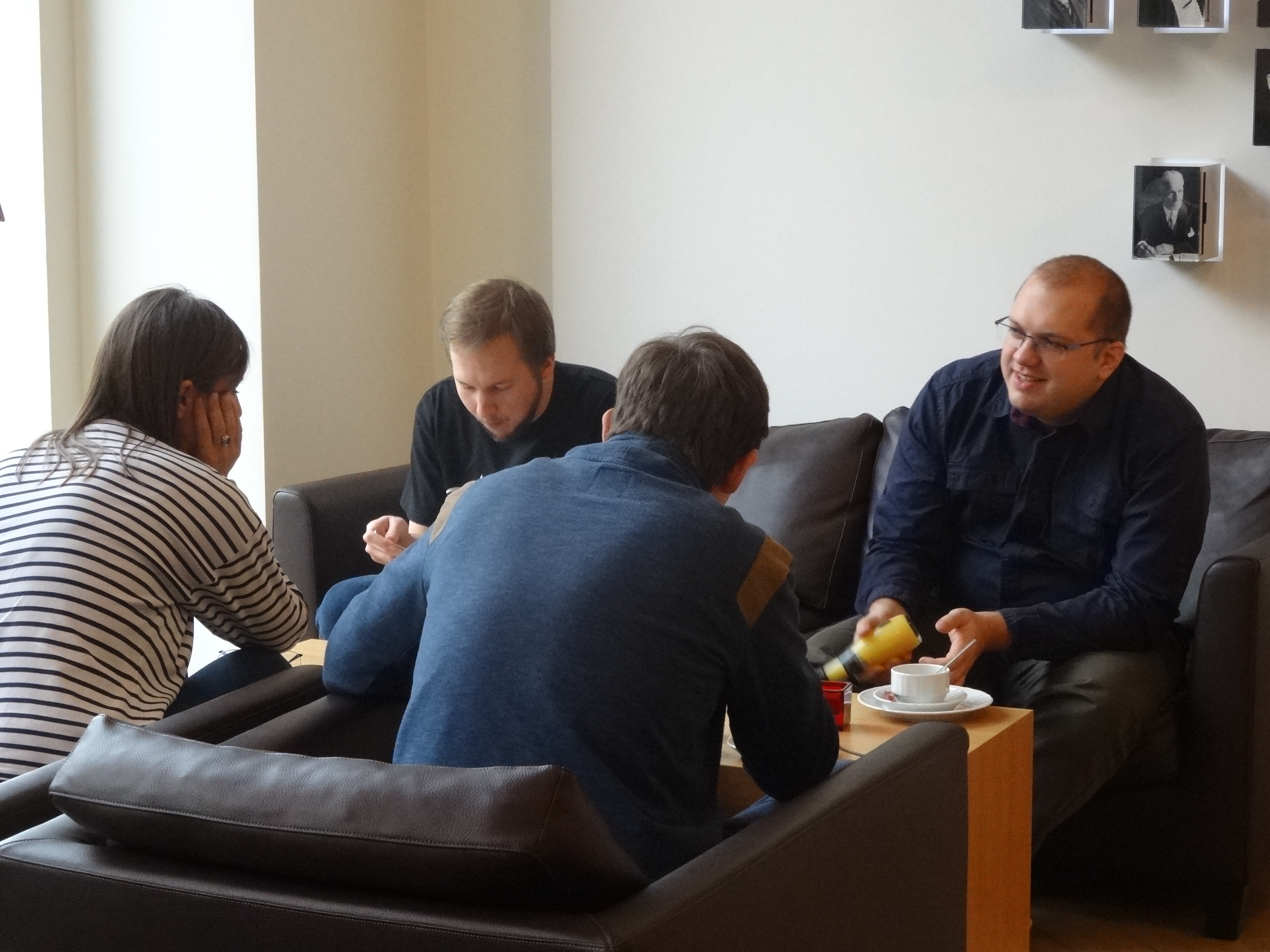
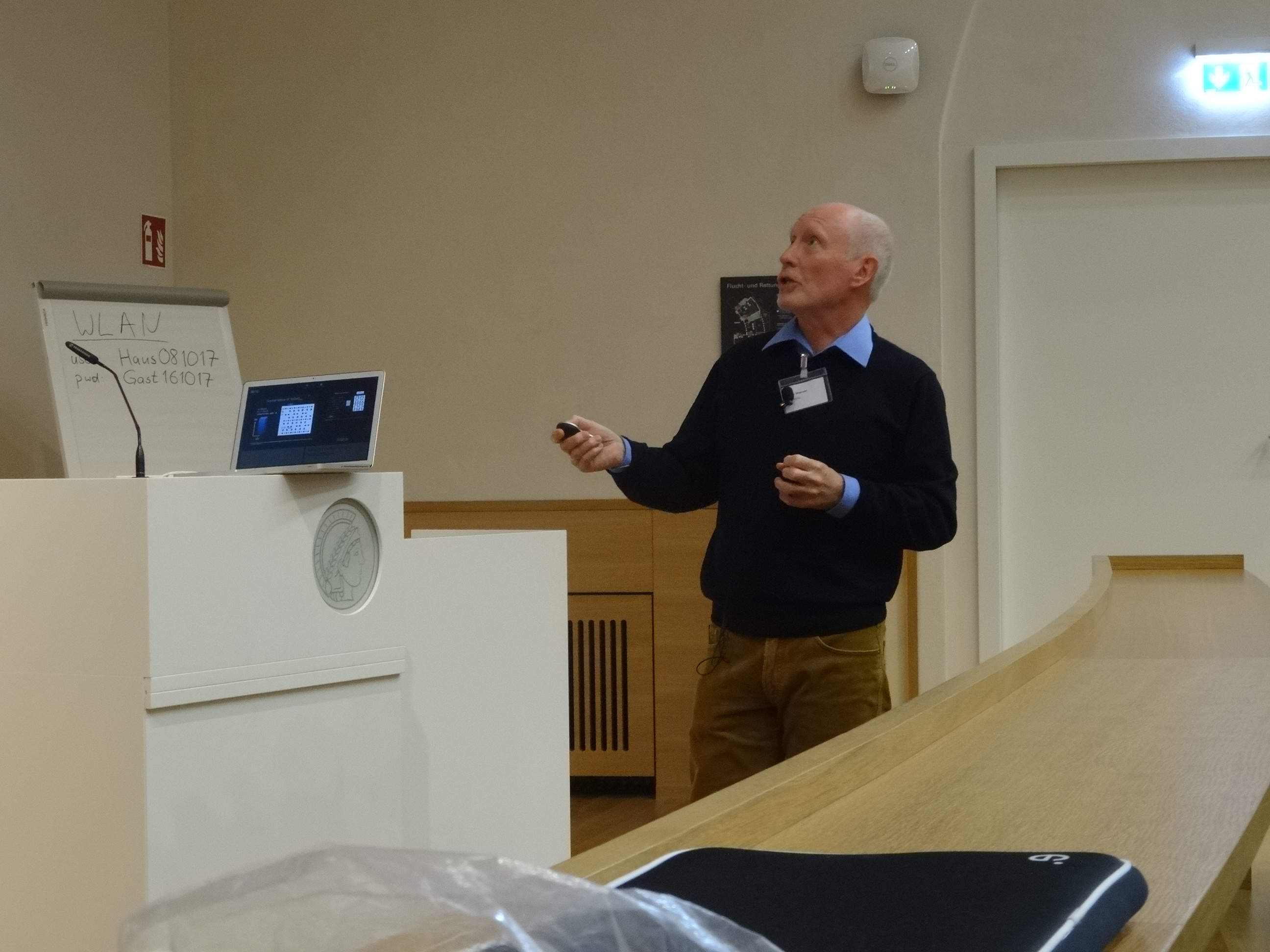
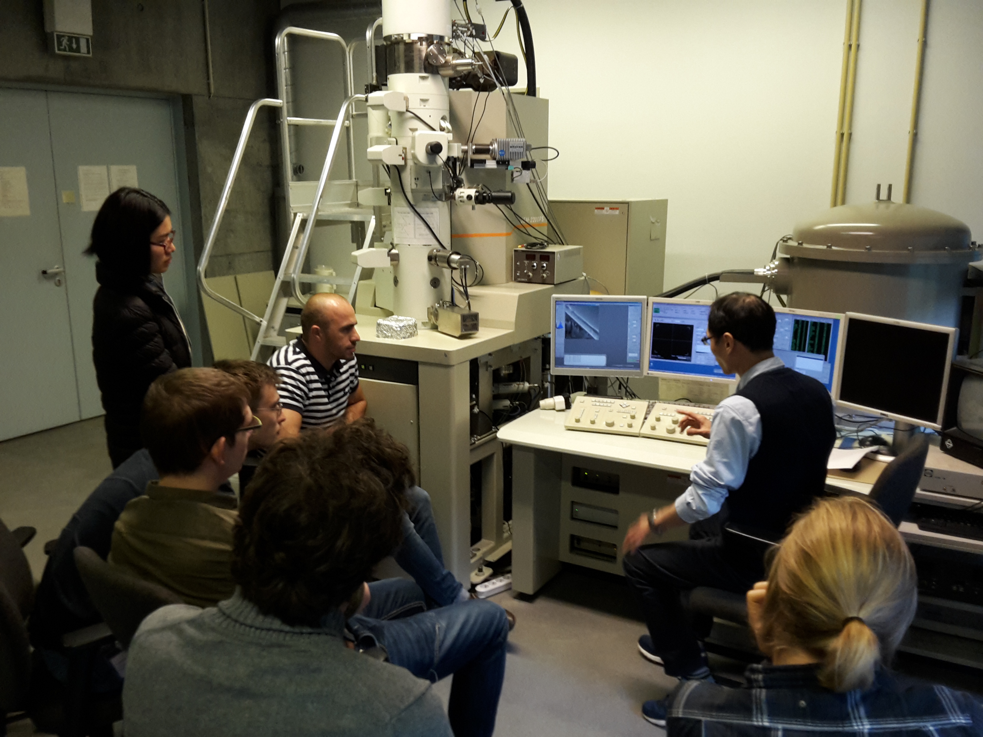
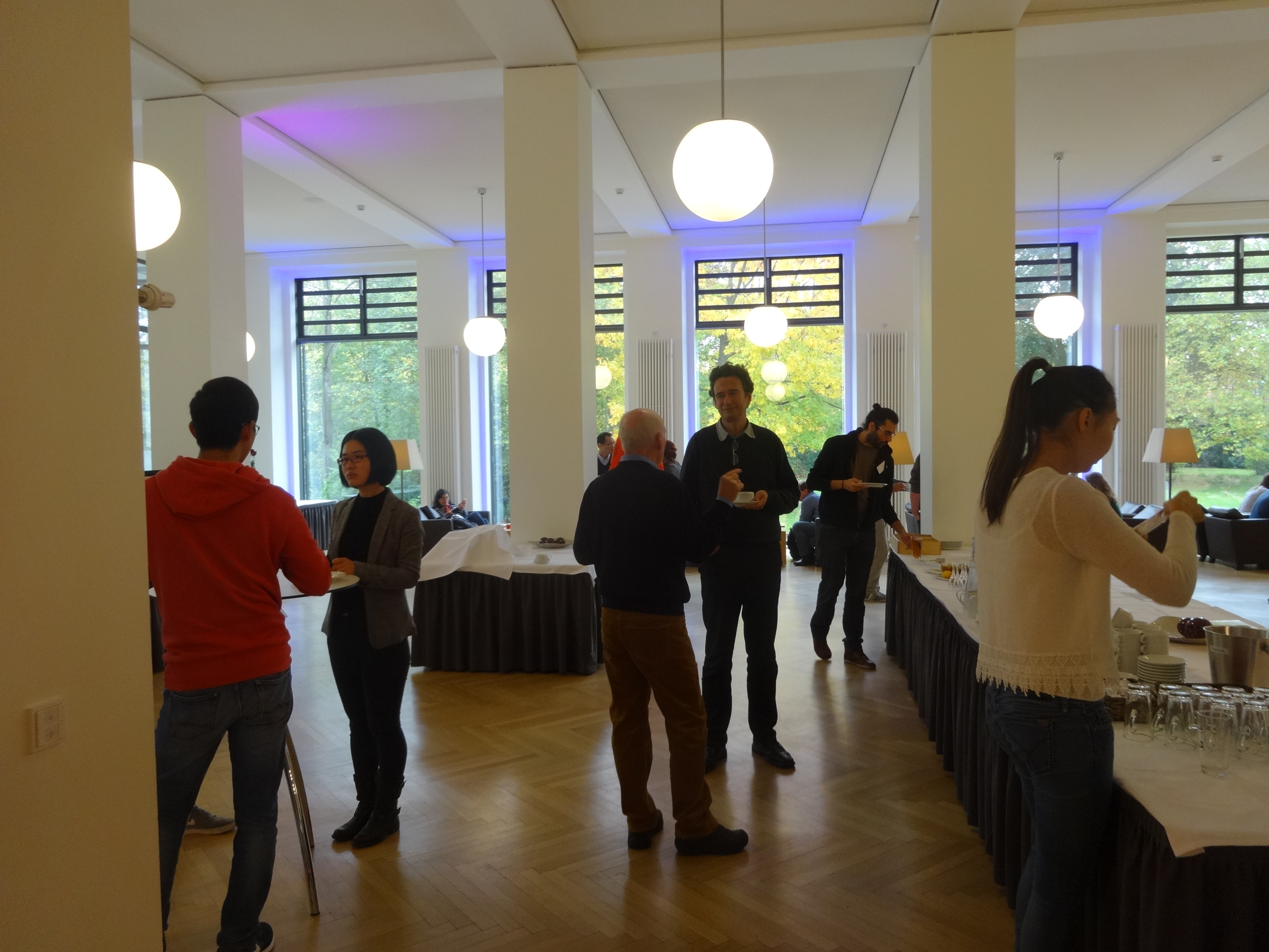
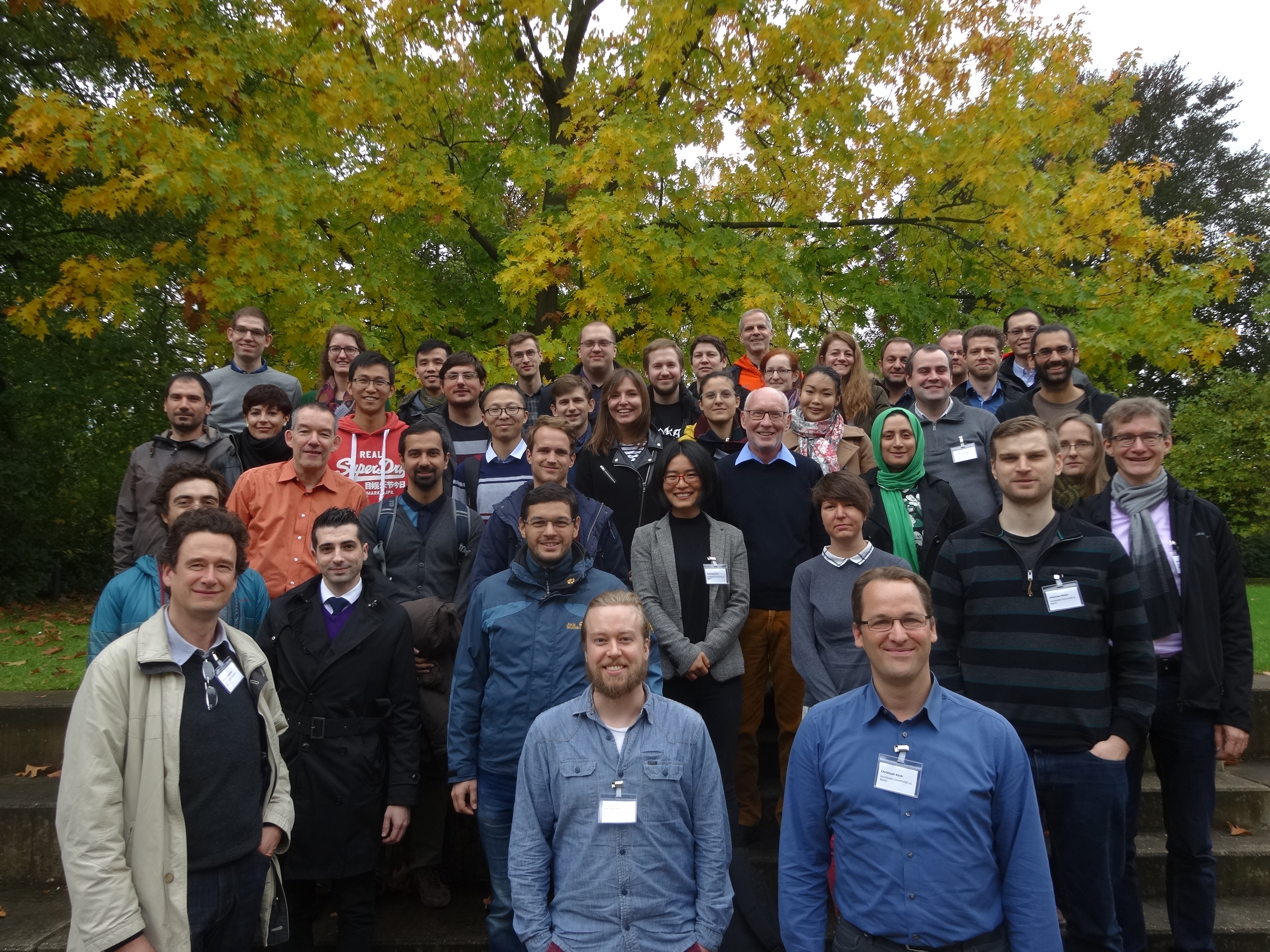
Pictures: