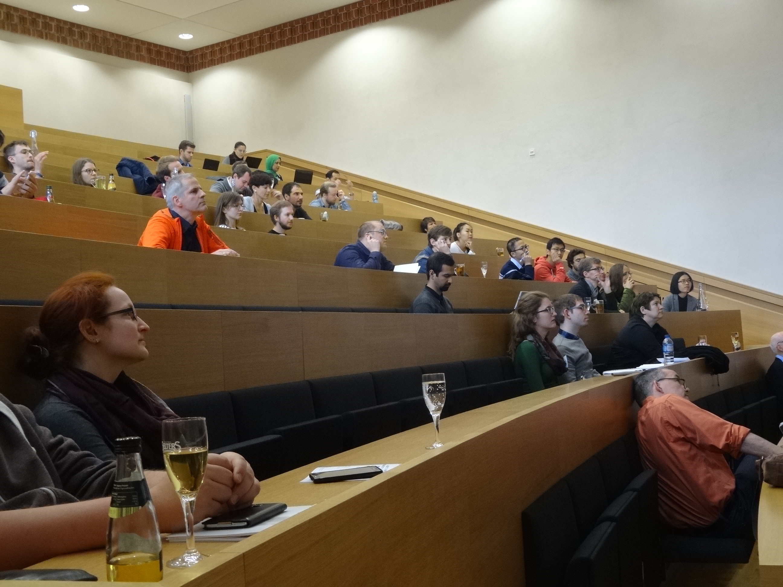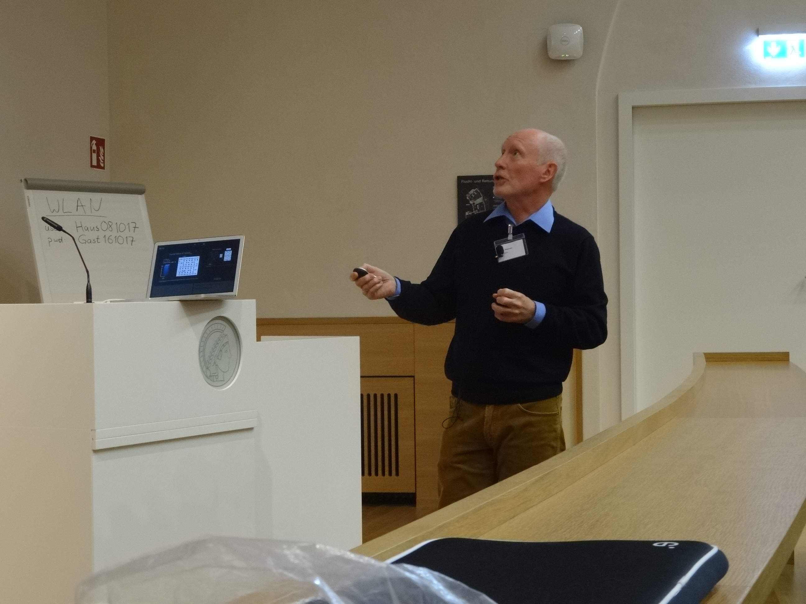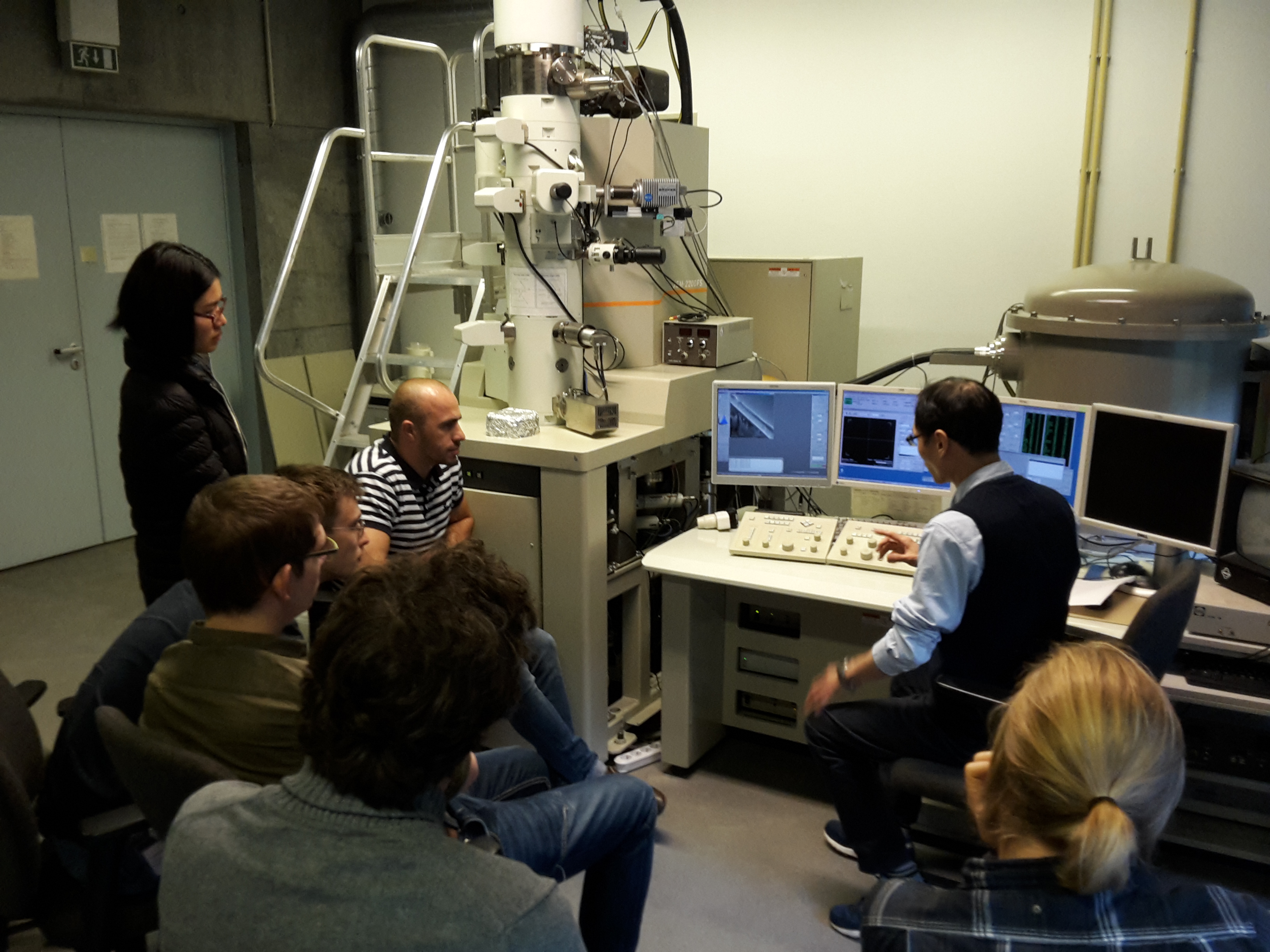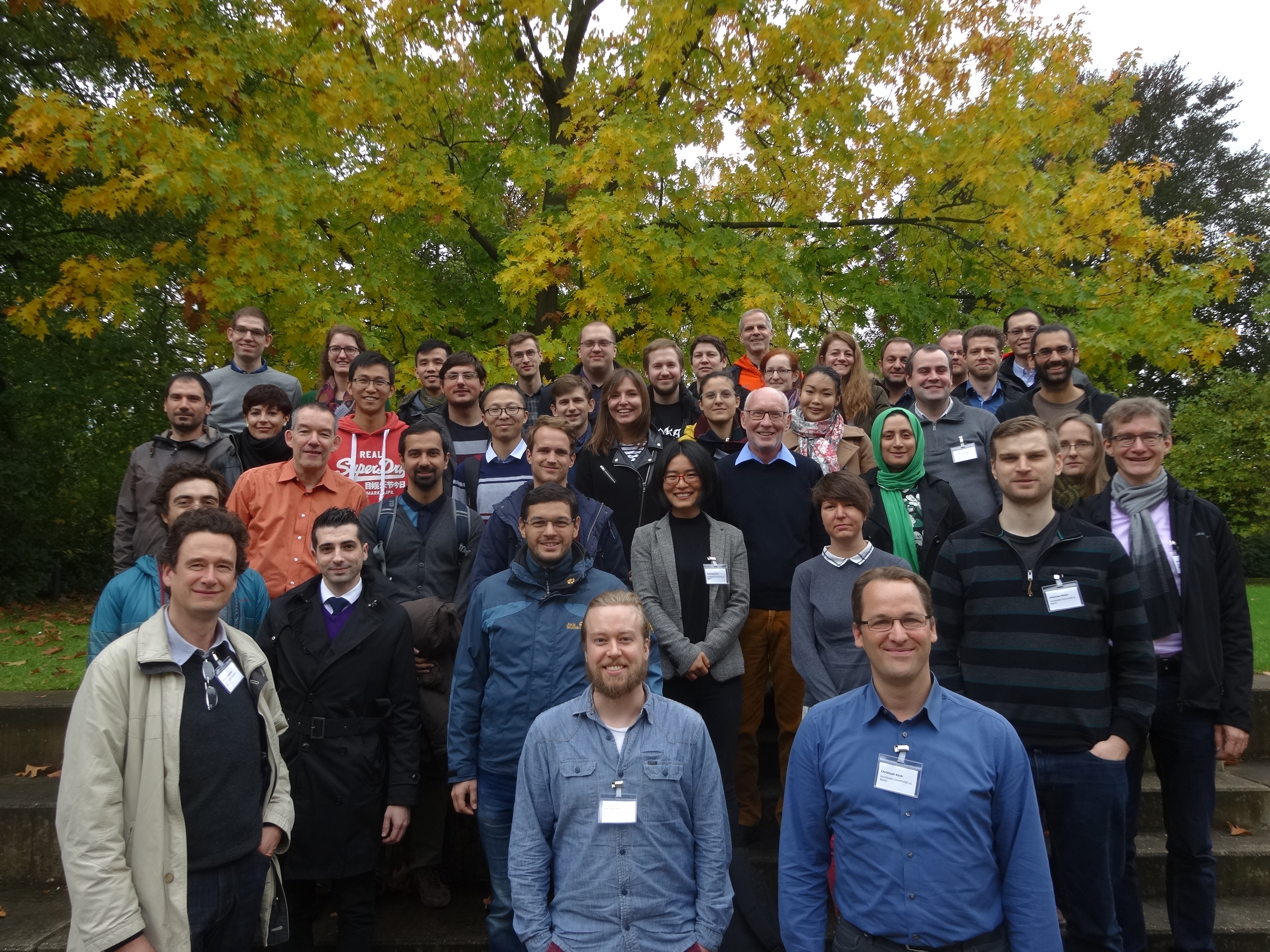
From October 9 through October 12, the autumn school on electron microscopy in materials science takes place at the Harnack House in Berlin. This school offers both practical courses as well as lectures on different aspects of modern electron microscopy.
Location: Harnack House in Berlin
Time: Monday, Oct 9, 9:00 am until Thursday, Oct. 12, 18:00
Programme: The programme for the school may be found here.
On Monday evening, participants are invited to present posters of their work (max. size: A0). Here ist the list of posters being presented.
Registration: The registration fee for participation in this workshop:
- € 100.00 for students (inkl. doctoral/PhD students) and
- € 150.00 for postdocs, etc..
This fee covers also snacks and beverages during coffee breaks as well as lunch at noon.
This school is organized and run by members of the following institutions (in alphabetical order):
- Fritz-Haber-Institut der Max-Planck-Gesellschaft (FHI)
- Helmholtz-Zentrum Berlin für Materialien und Energie (HZB)
- Humboldt Universität zu Berlin (HUB)
- Leibniz-Institut für Kristallzüchtung (IKZ)
- Max-Planck-Institut für Mikrostrukturphysik (MµP)
- Paul-Drude-Institut für Festkörperelektronik (PDI)
- Technische Universität Berlin (TUB)
Financial support for this school is provided by
- German Research Foundation / Deutsche Forschungsgemeinschaft
- German Society for Electron Microscopy / Deutsche Gesellschaft für Elektronenmikroskopie
- Thermo Fischer Scientific
- Carl Zeiss
![]()
![]()
![]()
![]()